
NVIDIA Hopper could be a 140 billion transistor GPU
Published: 09/02/2022 07:10
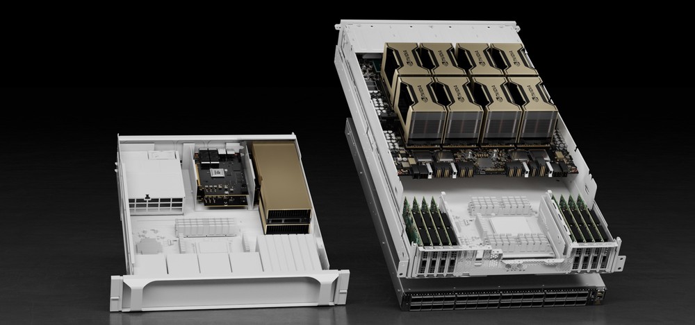
After the "misunderstanding" related to the filing of the name, NVIDIA's next-generation Hopper GPUs are back in the spotlight with interesting technical details regarding what will probably be the top of the range of the series, the infamous Hopper GH100. The latest news on the subject comes from the Chiphell forum and basically speak of what will be the flagship NVIDIA as regards the HPC, AI and Server segment, not gaming in other words.
In detail, they refer to a Hopper GPU with over 140 billion transistors, a real monster that would confirm previous rumours that it will probably be the most powerful and largest chip ever produced so far.
While there's no mention of the Hopper GH100 in this post, it's likely that NVIDIA is using the same scheme as seen in the Ampere family. Recall that Hopper GPUs will be produced on TSMC's 5nm node, the likely GH100 is credited with a surface area close to 900 mm² and will - like its competitors Intel Old Bridge and AMD Aldebaran - be based on a MCM (Multi-Chip-Module) design.
The premises for a substantial performance leap are all there, but what remains to be seen is the power consumption, which, from what we know, will not be at all contained despite the 5 nanometre technology.
Written by: Joshua Wilson